
Why is DFT important in ASIC flow?
By Liam Miller
Design for Test (DFT) is, in essence, a step of the design process in which testing features are added to the hardware. While not essential to performance, these features are key to tests undertaken as part of the manufacturing process to ensure that chips going to customer products are functioning correctly.
There are many benefits to DFT that become evident over the course of the design and manufacturing process. The first and most significant of these is the essential need for testability in any complex design, though effective DFT strikes a balance between thorough testing and the time required to run those tests.
Testing needs
While early, simple circuits with a handful of gates could be tested with relatively little test planning in the design process, modern ASICs are invariably far larger in complexity if not physical size and continue to become more so with each passing year. As the circuitry becomes increasingly complex, creating effective test programs after the design is implemented becomes increasingly challenging, time consuming and specialised. The step to incorporating the idea of testability into the design flow was an inevitable one as a matter of necessity, and so DFT has become ubiquitous.
When considering the potential for defects in any manufactured silicon, being able to reliably test produced chips is an essential part of ensuring the products delivered to customers perform to expected standards. Well-designed DFT elements will enable this while minimising the additional space and silicon taken by the testing logic, and test programs could not only identify whether a given chip is failing but also provide enough detail to help identify where the flaw is to be found.
Test time
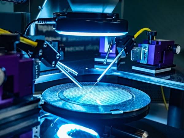
Flaws in the manufacturing of silicon are well-known by now, and with more complex designs using more advanced technology there is always more that can go wrong. There will always be a few chips that are flawed enough to be unsatisfactory, or even fail entirely. Testing for these chips is an essential step in ensuring the quality of the end-product.
Testing all those chips is, however, a time-consuming task. And like any task, that testing costs. Perhaps the tests take a matter of seconds but when multiplied across many chips, each second spent on a test has a distinct value. As such, test programs designed to make use of testing logic that have been added into the design specifically for this process can result in a significant reduction in the test time, resulting in large savings to test costs.
However, a DFT engineer must also consider the amount of time their own test features will consume. A perfect design that identifies and diagnoses every possible flaw in specific detail might not only take up greater space, but also increase the test time to a degree that ceases to be commercially viable. Ultimately this becomes a delicate balancing act of testing thoroughly enough for a design’s needs and not being so extensive that the design becomes financially infeasible.
What does DFT involve?
Now the case for the necessity of DFT has been made clear, what is involved in undertaking it? First must come an understanding of what an ASIC or part of ASIC is intended to do and how it has been designed to do so. Once this and any appropriate standards have been established, an approach can be determined based on the complexity and requirements.
What this involves can vary. Some techniques are relatively simple, such as introducing additional resets into a design that might allow a design to be brought into a known state more quickly for testing, though these are generally building blocks toward a larger strategy. More common techniques might include scan-based testing, built-in self-test or JTAG support to allow greater observation of behaviour and, consequentially, more information by which the nature of a fault might be identified.
When does DFT start?
As with any design feature, effective DFT implementation requires consideration from the beginning, an appropriate strategy being factored into early iterations of an ASICs architecture rather than making significant changes later. A DFT engineer might also conduct further analysis during the RTL design phase to help identify elements that might prove particularly helpful or detrimental, though the main bulk of DFT is typically inserted into a design later in the process. Once the architecture and RTL is largely established and verified, the DFT engineer can work with the design to incorporate the techniques they believe are most appropriate without having to worry about significant changes appearing in the system. As DFT will inevitably introduce a degree of additional logic, a physical design engineer will also need a strong impression of what DFT measures are planned from early in the process in order to begin incorporating it into the floorplan.
By the time a design reaches the foundry it will feature everything it needs for produced silicon to be tested quickly and efficiently, an effective application of DFT striking a balance between thoroughness, speed and information to help get the best yield.
Sondrel are currently hiring for DFT engineers with a range of experiences, if you have skills in this area then please check out our vacancies and apply here!