
Neon and Helium Tool Flows
Neon: Physical Design
Neon is the management side of the equation. It defines the steps, check points and stages all implementation projects go through.
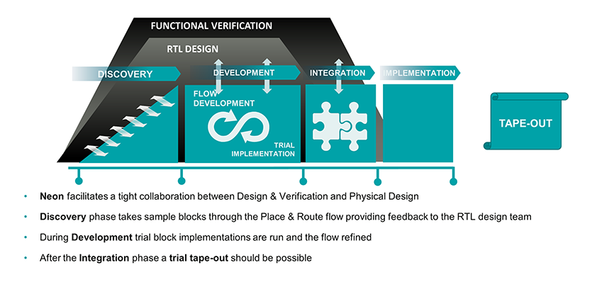
Physical chip implementation is categorised in 4 stages: Discovery, Development, Integration and implementation.
Early phases, run in parallel with RTL design and then Functional Verification (FV), is the time to get ready. By the end of integration, we can perform a trial tape out . This is a test to ensure all issues arising from variable in the flow with regards to tools, etc. are ironed out.
The implementation process is effectively automated for that chip and we know the tools can handle it. And at this stage, the RTL/netlists is final – bar any critical issues discovered by FV or caused by timing closure challenges.
During implementation, closing timing across all of the relevant timing scenarios and maintaining clean DRC checks are the critical task. Once we get to that point, the final finishing steps are run which add things like metal fill and seal rings. The timing and DRC/LVS checks get re-run and any issues introduced, e.g., metal fill not meeting required density or tweaking the timing, get resolved. Once we're satisfied that any remaining issues have been addressed or can be waived, we'll tape-out.
Helium - Re-configurable Design Flows
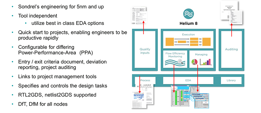
We use EDA tool sets from different vendors and have built intelligence into Helium to enable us to automatically switch as needs arise.