
How do you convert a design in FPGA to an ASIC?
By Charlie Passey

Why use an FPGA?
FPGA (field programmable gate arrays) are an integrated circuit which has the ability to be reprogrammed in order to work on different designs, differing from an ASIC (application specific integrated circuit), which as the name suggests, is application specific. FPGA’s are often chosen during a prototyping phase due to this programmability, ease of use, and although they have a high unit price compared to ASICs, they are much cheaper upfront. They also find use in applications where the higher cost of an FPGA is not the deciding factor, but instead their programmability, allowing for improved algorithms and designs to be implemented over time. However, what if you wanted to convert this design to an ASIC one?
Why would you want to convert?
There are multiple reasons why you might want an ASIC over an FPGA. Production volume, efficiency, budget, time to market and customisation are all areas that are considered when making this decision. Both FPGA and ASIC designs are specified by a hardware description language such as Verilog or VHDL, however it is not quite a simple copy and paste to convert one to the other. Areas such as power grids, clock trees, I/O placement, floor planning, layout and routing are all automated by synthesis in an FPGA design, however, need to be taken care of in an ASIC design, often by different specialist workers. Conveniently, because both designs rely on HDL scripts, traditional ASIC design flow can be applied for this conversion, however there is some extra work that needs to be carried out first. FPGA RTL is often written with FPGA libraries, so taking the code and plugging it straight into an ASIC design may not necessarily work. There is also the fact that FPGA RTL and ASIC RTL may be written to different standards, as an FPGA is more forgiving for retrying design.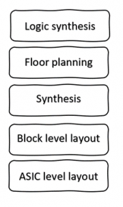
Another aspect to consider is that FPGA’s tend to come with some hardened IP already, CPU’s, DDR components along with PHYs or Serdes which can allow the user to build onboard controllers for different interfaces, USB, PCIe and SATA for example. With an ASIC you would need find the suitable Serdes and PHYs for the desired technology, integrate them into your design and then verify to ensure that all of this works with the digital logic that is being used to drive the interface. Because FPGAs are programmable, they can be vulnerable to reverse engineering and hacking. ASICs are much more difficult to reverse engineer, making them a more secure option for sensitive applications. If you have a proprietary FPGA design that you want to protect, converting it to an ASIC can make it much more difficult for others to copy or steal your design.
There is also the aspect of performance analysis to consider. If you are testing an FPGA system, and during this you find a bottleneck, then you are able to try different fixes until that works, with an ASIC, this is not possible, which is why there is such an emphasis on performance analysis and modelling, and even emulating the design.
The ASIC design flow
A typical ASIC design flow that one might take their RTL through is as follows:
The first step of this would be logic synthesis, which is the step where our register transfer level design (RTL) is tuned into a design in terms of logic gates.
From here, the next process would be floor planning where we layout the general shape and size of our design, place down the input and output pads and any macros so that the routing space in between everything can be determined.
After this step, next up would be synthesis where timing constraints, static timing analysis and optimisation are carried out. At this point the placement, power and clock planning are all updated.
An ASIC design can be split into several sub-circuits, with each of these sub-circuits being referred to as blocks. The step after synthesis is block level layout, where these blocks are placed into the design and the routing for them is determined.
The last step would be the ASIC level layout, where the ASIC integration of all blocks and the placement and routing are carried out. It is also at this point that the GDSII file is created which provides a graphical representation of the design.
Next steps
At this point, with the GDSII file produced, the work on the design can be concluded and sent off for tape out and production. Once this stage is finished and returned, then the focus can be shifted on to bring up and characterisation process, where if done in a diligent and thorough way will give the customer confidence in the reliability of the final product.
Conclusion
Overall, converting an FPGA design to an ASIC can provide several benefits, including cost savings, better performance, lower power consumption, increased security, and intellectual property protection. However, the conversion process is complex and requires specialised expertise, so it's important to carefully weigh the costs and benefits before deciding to proceed. ASIC design teams typically consist of engineers with experience in digital design, physical design and verification.
If you are thinking about converting an FPGA to an ASIC and require outside specialised knowledge and expertise then you would be in safe hands with Sondrel. We are experts in ASIC design and supply and can offer a full turnkey service from concept architecture to silicon supply. You can find out more about our solutions here.