
Describing the ASIC physical design flow
By Elliot Smythe
Design Specification
The design specification is the most important step in the design flow as it details anything that needs to be considered or strict requirements that need to be met when designing the ASIC, these include; functionality, inputs and outputs, performance, space and power budgets, corner cases, future modifications to the design. The requirements for each of these sections allow the architects to develop the target architecture, the clarity of the specification is key and a skilled architect will ensure there is no ambiguity in the design ensuring the ideas of the designers and customers are aligned.
This dictates what the design is verified against at the end of the process to indicate a successful product and so should be thoroughly reviewed and modified alongside the stakeholders.
Once the specification is handled, the design entry begins.
IP
Intellectual property are used when identical systems are required and repeated in designs, these are usually process that use universal standards such as USB or commonly used functions that can be delivered in IP as a re-use strategy. IP can come with a scripting engine that tailors a general use IP to your specific use case, so there should be no need to change the internal logic of the IP from the user.
As these would require a lot of work to create each time they are used in a design general intellectual property blocks, or cores, are used and configured for the specific use case within each design. They can come in three forms of completeness;
- Soft IP
- HDL code for the IP, this is the most flexible option and requires the most work
- Netlist-only
- Netlist for the IP, this is used in the implementation but doesn’t include the source code for the design, this offers no code flexibility but offers freedom for place and routing.
- Hard IP
- The floor planned architecture-specific netlist is provided, this is the least flexible option and requires the least amount of work, and the shape of the placed design is not alterable so may result in a larger floor area when implemented as opposed to using a netlist only design.
When implementing the IP blocks, instantiation templates and simulation models are needed, these are used for connecting the ports of the block and testing system. IP is typically purchased from vendors, or IP blocks are used from internal company resources, with high complexity IP having licenses. Another option is open source IP, these come at the cost of having to be verified in house due to the risk of open source and so is not commonly used in industry. These IP will be comparable with different devices or will be made for specific architecture, and include data sheets detailing topics such as signaling, performance, and design options.

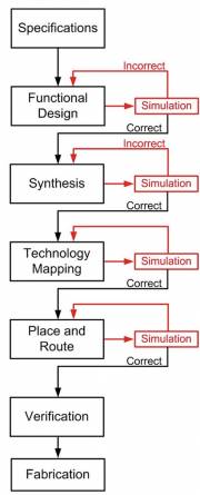
Functional Design
The front end team creates a top level design to meet the specification, separated into data path and control logic. The data path is the movement of data around the system, whereas the control logic controls the operation of the system.
The micro-architecture is then implemented in RTL by translating the design into a hardware description language, or HDL of the system. Each module and sub-module is designed conforming to the architecture of the design, containing combinatorial and synchronous blocks to implement the desired behaviour. The RTL developed modules are then instantiated and connected forming the full design.
Alternate approaches to functional design
High level synthesis tools can be used to convert high level code into HDL. These can convert from languages; such as C by parallelising parts of loops in programs, Simulink model designs, and specialized languages such as OpenCL-HDL. All of these produce HDL that then are carried to the next step.
Functional Verification
Functional verification is an iterative process which occurs throughout the functional design process to test the HDL to ensure it meets specification. Verification is performed in a hierarchical manor beginning with low level modules. Once when they are shown to be verified and functional, subsystems at the next level of the hierarchy are verified, then following this the top level. Verifying in a hierarchy reduces testing time as when testing higher level modules for bugs, an error could be causes by any one of its lower level modules that is being used, taking more time to identify the cause of the error. When starting with the modules with the least sub modules errors can be identified easier, also allowing the more top level modules to be tested with a guarantee of sub module functionality.
At checkpoints through the HDL design process synthesis is ran. This is to allowing the pipelining of the two functionally consecutive tasks, details such as the clocking, busses and registers can be synthesised to check the design before the final HDL is formed. It also illuminates the timing and area for the initial circuit. If the circuit is over timing requirements or area before the completed design there is a high chance it will not meet the required timing constraints once completed, allowing the design to be re-assed earlier in the HDL stage.
Synthesis
The function of the synthesis is to convert the high level RTL description to a netlist which is a set of logic gates and connected components. In this process the behaviour and combinational blocks are turned into valid circuits, and minimised respectively. Hardware structures such as multiplexers and memory are set and simple equivalent circuits are generated from numerical operators.
Mapping
Each node in the netlist is then mapped to the available cells in a cell library in order to build the design, creating a technology specific logic description from the netlist.
Synthesis verification
The pre-layout netlist is then verified to ensure the circuit conforms with the design specification by taking initial estimates of timing and device area. It is also checked the code is all synthesised correctly and no code was optimised away. These problems can be resolved in the synthesis tool settings.
Place and route
All of the cells in the architect-specific netlist need to be floor planned and the connections are then routed, this is the most computing intense and time expensive section in the design flow because it takes multiple iterations for automatically generated connections to find a configuration to meet timing requirements. Test logic is also inserted into the design to allow for the testing and debugging when the circuit is fabricated, however this can also be done at the RTL stage.
Timing Verification
Timing verification involves comparing simulated timing against specification. It can be reduced by examining critical paths, then the final design is simulated in a testbench. This provides the user with a working design that meets the design constraints. (is a bitstream only generate with fpgas, is it also tested on FPGAs after test bench simulation or not)
Fabrication
The final design is then fabricated, the placed design is etched onto silicon and packaged before being shipped to the customer. The fabricated ASIC then undergoes a series of tests to ensure the theoretical design was executed correctly and that the finish product meets specification. Approximately 60% of fabricated ASICs are not fully functional first time, and as fabricating is an extremely expensive process the verification at each stage needs to be vigorous. If an error is found with the ASIC, changes are made, and it is re-fabricated. Because of the expense when fabricating, “test prints” on multi-project wafers are made for a small sample size to check the functionality before printing on mass, however this is still very costly.
Figure 1 LaMeres B.J. (2019) The Modern Digital Design Flow. In: Quick Start Guide to VHDL. Springer, Cham.
About Sondrel™
Founded in 2002, Sondrel is the trusted partner of choice for handling every stage of an IC's creation. Its award-winning define and design ASIC consulting capability is fully complemented by its turnkey services to transform designs into tested, volume-packaged silicon chips. This single point of contact for the entire supply chain process ensures low risk and faster times to market. Headquartered in the UK, Sondrel supports customers around the world via its offices in China, India, France, Morocco and North America. For more information, visit www.sondrel.com/careers